15. September 2020 | Press Release
Record efficiency of highly efficient III-V multi-junction solar cells on silicon / High energy efficiency at attractive cost
Herzogenrath, Germany, September 15, 2020 – A central stage in the development of economic solutions for the industrial use of multi-junction solar cells for power generation has been reached. For the first time, an efficiency of 25.9 percent has been achieved with a multi-junction solar cell grown directly on a silicon substrate.
This record figure was achieved by researchers at the Fraunhofer Institute for Solar Energy Systems ISE in close cooperation with the Technical University of Ilmenau, the Philipps University of Marburg and the epitaxy experts at AIXTRON SE, a leading provider of deposition equipment for the semiconductor industry, as part of the funded "MehrSi" project. The team, together with scientists from the Fraunhofer ISE, succeeded in optimizing the layer structure and technology.
Key technology tandem photovoltaics
"For the first time we have now been able to realize a tandem solar cell based on a silicon wafer with such high efficiency," comments Dietmar Schmitz, Vice President Corporate Technology Transfer at AIXTRON SE. Until now, the production of III-V multi-junction solar cells has been based on a more expensive substrate material, for example also a compound semiconductor material.
Dietmar Schmitz emphasizes what is special about this basic research: "The gallium and phosphorus atoms must occupy the correct lattice positions at the interface with silicon. To achieve this, we have to control the atomic structure very well. This requires exceptionally high precision. In addition, to achieve the necessary high quality of the epi-wafers, it is crucial that a high crystal quality of all layers is achieved during epitaxial growth. This was achieved in the project thanks to the improved system technology developed by AIXTRON and the good cooperation with the project partners".
Low price – High cost attractiveness of silicon wafers
In this so-called tandem photovoltaics, different combinations of high-performance solar cell materials are arranged in layers on top of each other in order to use the different wavelengths of sunlight more efficiently when converting light into electrical energy. Silicon is suitable for absorbing the infrared portion of the sunlight spectrum. Layers of different III-V semiconductor compounds, a few micrometers thick, are then applied to the silicon base to convert the ultraviolet, visible and near-infrared light more efficiently into electricity. Tandem photovoltaics is a key technology for the energy transition. Due to the silicon used, the multi-junction solar cells grown on a silicon substrate are more cost-effective than solar cells based on other substrates.
Work on faster crystal growth to further reduce manufacturing costs
From the technological basis that has now been achieved, the alliance partners are working at high pressure to further increase efficiency and reduce manufacturing costs. To this end, the deposition of the layers is to be realized even faster, with higher throughput and thus more cost-optimized. In addition, the efficiency of the solar cells is to be further improved.
"Specifically, the dislocation density in the III-V solar cell layers is to be reduced from 108 cm-2 to the range of 1-5*106 cm-2 in order to increase the efficiencies to more than 30 percent. And last but not least, the cost-effectiveness of the epitaxy processes is to be further optimized," explains Prof. Dr. Michael Heuken, Vice President Corporate Research and Development at AIXTRON SE.
By means of more cost-effective processes in combination with silicon as the lowest sub-cell, tandem technology is to be made accessible for broad-based photovoltaics in the future. AIXTRON has already been working on such III-V multi-junction solar cells on silicon with several partners for many years.
The project "SiTaSol" for the joint development of layer packages that can be produced as quickly and cheaply as possible is funded by the EU. In "SiTaSol" AIXTRON has built and tested a specially optimized Metal Organic Chemical Vapor Phase Epitaxy (MOVPE) system in its own laboratory.
Further information about tandem photovoltaics at www.ise.fraunhofer.de/en.html
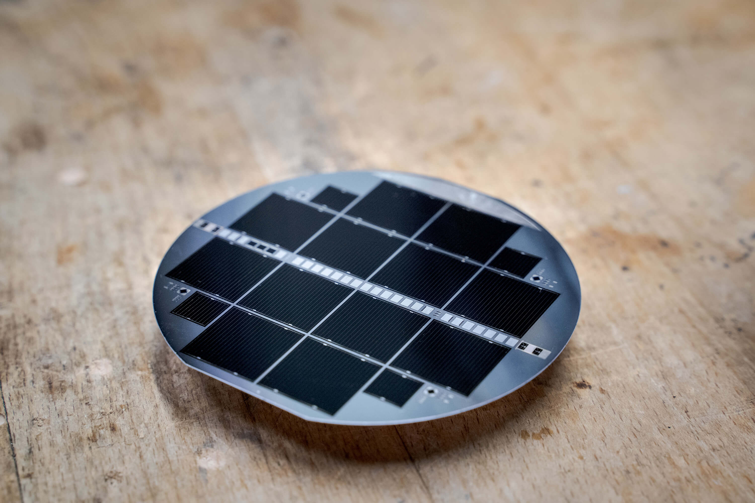
To download a photo (Several III-V tandem solar cells on a silicon substrate with 10 cm diameter © Fraunhofer ISE /Photo: Markus Feifel) please click here.
The project "SiTaSol" is funded by the EU (funding number: 727497) and the project "MehrSi" by the Federal Ministry of Education and Research BMBF (funding number: 03SF0525D).
Our registered trademarks: AIXACT®, AIXTRON®, Atomic Level Solutions®, Close Coupled Showerhead®, CRIUS®, EXP®, EPISON®, Gas Foil Rotation®, Optacap™, OVPD®, Planetary Reactor®, PVPD®, STExS®, Trijet®
Alan Tai
Taiwan/Singapore
Christof Sommerhalter
USA
Christian Geng
Europe
Hisatoshi Hagiwara
Japan
Nam Kyu Lee
South Korea
Wei (William) Song
China
AIXTRON SE (Headquarters)
AIXTRON 24/7 Technical Support Line
AIXTRON Europe
AIXTRON Ltd (UK)
AIXTRON K.K. (Japan)
AIXTRON Korea Co., Ltd.
AIXTRON Taiwan Co., Ltd. (Main Office)
AIXTRON Inc. (USA)
Christoph Pütz
Senior Manager ESG & Sustainability
Christian Ludwig
Vice President Investor Relations & Corporate Communications
Ralf Penner
Senior IR Manager
Christian Ludwig
Vice President Investor Relations & Corporate Communications
Prof. Dr. Michael Heuken
Vice President Advanced Technologies