11. April 2012 | Nanotechnology
AIXTRON SE today announced that its BM 300 system has been successfully started up at the National Institute of Advanced Industrial Science and Technology (AIST) in Japan. The system was installed in 2011 in AIST’s super cleanroom facility in Tsukuba and was commissioned by the local AIXTRON support team. Dr. Shintaro Sato, group leader at AIST, presented the growth results on April 10 at the 2012 MRS Spring Meeting.
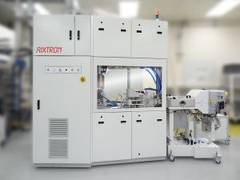
AIXTRON BM 300 with automated wafer handler
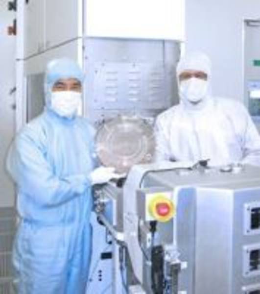
Fumio Yoshida and Andy Newham (AIXTRON) holding a 300mm wafer with graphene
“With the demonstration of monolayer graphene growth on 300mm wafers at AIST, we have achieved a significant milestone,” comments Dr. Ken Teo, Director of Nanoinstruments at AIXTRON. “The BM 300 is the most technologically advanced platform for graphene production available, incorporating a sophisticated gas delivery system for precise precursor delivery, ARGUS in-situ wafer thermal mapping, a high uniformity wafer heater and an automated handling system. The ability to deposit graphene with a high degree of controllability and repeatability onto 300mm wafers is an essential step in enabling large wafer-scale integration of graphene, and paves the way for exploiting the unique properties of graphene in next generation semiconductor devices.”
Dr. Sato’s team at AIST will use the system to deposit high-quality graphene with a controlled number of layers. This will be a key part of a process technology used for creating low-voltage operation CMOS FETs, in which the power supply voltage will be less than 0.3V.
The research is backed by the Funding Program for World-Leading Innovative R&D on Science and Technology (FIRST), which aims to encourage cutting-edge research and development that will strengthen Japan’s international competitiveness and contribute to society and people’s welfare by sharing the results. The FIRST Program was approved by the Council for Science and Technology Policy, Cabinet Office, Government of Japan in 2009, and is being operated by the Cabinet Office, Government of Japan and the Japan Society for the Promotion of Science (JSPS). The wafer processing is being carried out at AIST’s Collaborative Research Team Green Nanoelectronics Center (GNC) within the research project ‘Development of Core Technologies for Green Nanoelectronics’ (core researcher Dr. Naoki Yokoyama), which has been adopted for the FIRST Program. The GNC was established in April 2010 and comprises researchers from both research and industry.
Our registered trademarks: AIXACT®, AIXTRON®, Atomic Level Solutions®, Close Coupled Showerhead®, CRIUS®, EXP®, EPISON®, Gas Foil Rotation®, Optacap™, OVPD®, Planetary Reactor®, PVPD®, STExS®, Trijet®
Christian Ludwig
Vice President Investor Relations & Corporate Communications
Alan Tai
Taiwan/Singapore
Christof Sommerhalter
USA
Christian Geng
Europe
Hisatoshi Hagiwara
Japan
Nam Kyu Lee
South Korea
Wei (William) Song
China
AIXTRON SE (Headquarters)
AIXTRON 24/7 Technical Support Line
AIXTRON Europe
AIXTRON Ltd (UK)
AIXTRON K.K. (Japan)
AIXTRON Korea Co., Ltd.
AIXTRON Taiwan Co., Ltd. (Main Office)
AIXTRON Inc. (USA)
Christoph Pütz
Senior Manager ESG & Sustainability
Christian Ludwig
Vice President Investor Relations & Corporate Communications
Ralf Penner
Senior IR Manager
Christian Ludwig
Vice President Investor Relations & Corporate Communications
Prof. Dr. Michael Heuken
Vice President Advanced Technologies