24. July 2012 | Press releases
5x200 mm GaN-on-Si Technology for the AIX G5 Reactor Platform
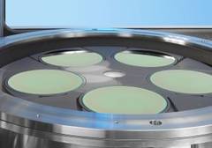
With its latest product, AIX G5+, AIXTRON SE has introduced a 5x200 mm GaN-on-Si (Gallium Nitride on Silicon) technology package for its AIX G5 Planetary Reactor platform. Following a customer-focused development program, this technology was designed and created in AIXTRON’s R&D laboratory and consists of specially designed reactor hardware and process capabilities. It is now available as a part of the AIX G5 product family and any existing G5 system can be upgraded to this latest version. Details of G5+ have already been disclosed to some of AIXTRON’s key customers.
“GaN-on-Si technology is a hot topic for MOCVD users and manufacturers today”, states Dr. Rainer Beccard, Vice President Marketing at AIXTRON. “It is the technology of choice for the emerging power electronics market segment, and also a very promising candidate for future high performance and low cost High Brightness LED manufacturing. The wafer size and material plays a crucial role when it comes to cost effective manufacturing processes, and thus the transition to 200 mm Standard Silicon wafers is a logical next step on the manufacturing roadmaps, as it offers unique economies of scale.”
”Being convinced that uniformity and yield are the key success criteria in 200 mm GaN-on-Si processes, AIXTRON conducted a dedicated R&D program”, adds Dr. Frank Wischmeyer, Vice President and Program Manager Power Electronics at AIXTRON. “We started the development process by conducting an extensive simulation program, which enabled us to design fundamentally new hardware components that provide unique process performance in our 5x200 mm processes, while still being compatible with the well-proven AIX G5 reactor platform.” The results are extremely stable processes, providing much better uniformity of material properties and enabling higher device yield than any other MOCVD platform, whilst offering a reactor capacity of 5x200 mm.
Some initial feedback from customers confirms the success of this technological development. Many of them have noted in particular that the fully rotationally symmetrical uniformity pattern on all five 200 mm wafers, the use of standard thickness silicon substrates and the controlled wafer bow behavior is exactly what they require for silicon-style manufacturing. “This uniformity pattern has been an inherent feature of AIXTRON’s Planetary Reactor technology, which we can now successfully obtain on 200 mm GaN-on-Si-wafers”, underlines Dr. Wischmeyer.
Our registered trademarks: AIXACT®, AIXTRON®, Atomic Level Solutions®, Close Coupled Showerhead®, CRIUS®, EXP®, EPISON®, Gas Foil Rotation®, Optacap™, OVPD®, Planetary Reactor®, PVPD®, STExS®, Trijet®
Christian Ludwig
Vice President Investor Relations & Corporate Communications
Alan Tai
Taiwan/Singapore
Christof Sommerhalter
USA
Christian Geng
Europe
Hisatoshi Hagiwara
Japan
Nam Kyu Lee
South Korea
Wei (William) Song
China
AIXTRON SE (Headquarters)
AIXTRON 24/7 Technical Support Line
AIXTRON Europe
AIXTRON Ltd (UK)
AIXTRON K.K. (Japan)
AIXTRON Korea Co., Ltd.
AIXTRON Taiwan Co., Ltd. (Main Office)
AIXTRON Inc. (USA)
Christoph Pütz
Senior Manager ESG & Sustainability
Christian Ludwig
Vice President Investor Relations & Corporate Communications
Ralf Penner
Senior IR Manager
Christian Ludwig
Vice President Investor Relations & Corporate Communications
Prof. Dr. Michael Heuken
Vice President Advanced Technologies